The Technology section is published with the support of Favbet Tech

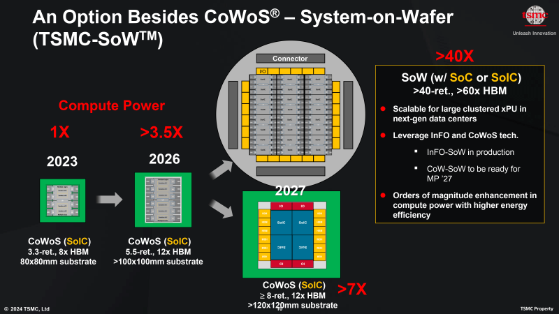
The record for the largest chip size sounds like something dubious, but it’s not case of TSMC. The company introduced chip-on-wafer-on-substrate (CoWoS) packaging technology, which will allow it to create systems-in-package (SiP) that are many times larger than the existing NVIDIA B200 or AMD Instinct MI300X processors. The processors will have monstrous dimensions of 120 x 120 mm and will consume kilowatts of energy.
“CoWoS®, SoIC and System-on-Wafer (TSMC-SoW™): TSMC's on-wafer-on-wafer (CoWoS) chip has become a key enabler of the artificial intelligence revolution , allowing customers to use more processor cores and high-bandwidth memory (HBM) stacked side by side on a single intermediate device. At the same time, our System on Integrated Circuits (SoIC) has established itself as a leading solution for 3D chip stacking, and customers are increasingly combining CoWoS with SoIC and other components for maximum system-on-package (SiP)
With System-on-Wafer, TSMC is offering a revolutionary new option that enables a large array of dies on a 300mm wafer, offering more processing power while occupying much less data center space and improving performance per watt by orders of magnitude. TSMC's first SoW offering, a logic wafer based on Integrated Fan-Out (InFO) technology, is already in production. A chip-on-wafer version using CoWoS technology is planned for 2027, allowing the integration of SoICs, HBMs and other components to create a powerful wafer-level system with processing power comparable to a data center server rack or even an entire server.”

The platform uses the InFO_SoW technology previously developed by the company, which allows the creation of large chips, as well as System on Integrated Chips (SoIC) technology. Another technology, Chip-on-Wafer (CoW), allows memory or other elements to be placed on top of the system.
In fact, we are talking about processors comparable in size to an entire 300 mm silicon platinum, which will allow placing a huge number of cores. This core packaging method will provide increased performance and energy efficiency through high speeds between components. Internally, the system will have low latency between cores and low resistance when transferring power. Unlike previous technologies, CoWoS allows the use of various technical processes and high-speed memory HBM4.
in the chip layout Course English For IT: Communication from Enlgish4IT. Make it easy to work and collaborate with multicultural teams and international clients. Take a 10% discount with promo code ITCENG. Information about the course
Sources: TSMC, Tom`s Hardware
The Technology section is published with the support of Favbet Tech


Favbet Tech is IT a company with 100% Ukrainian DNA, which creates perfect services for iGaming and Betting using advanced technologies and provides access to them. Favbet Tech develops innovative software through a complex multi-component platform that can withstand enormous loads and create a unique experience for players. The IT company is part of the FAVBET group of companies.
